Application Notes, February 2025
Trench Lining for Semiconductor Manufacturing
Sputter deposition is an important coating method for semiconductor chips. In a Damascene manufacturing sequence, sputter deposition is tasked to line nanoscale trenches and vias with thin metal layers, which serve the purpose of diffusion barrier, adhesion, and seed for subsequent trench filling.
Various trench-lining techniques have been under development for over two decades. New processes and equipment have been introduced to meet the challenges. Today, practical methods often employ special hardware to bring together several physical phenomena, including:
- Ionization of atomic species in front of the substrate;
- Acceleration of ionic species towards the substrate;
- Etching/re-sputtering of deposited material;
- Redeposition of sputter-etched material on trench facets;
- Shadowed vapor deposition on trench facets;
- Reflection, or non-sticking, of large-incident-angle species;
- Thermal induced atomic migration.
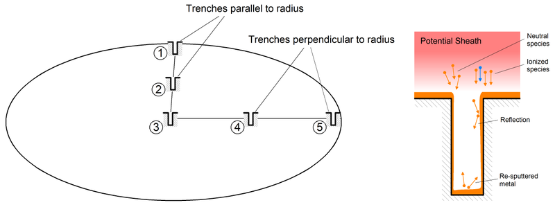
Tin Model’s PVD modeling tool sets, V-Grade 5S, can be used to aid and expedite the development of trench-lining technology. In the following, we show simulation of a sputter deposition, incorporating the above elements, for lining nanotrenches (aspect ratio = 3) on a semiconductor wafer of 20 cm in diameter.
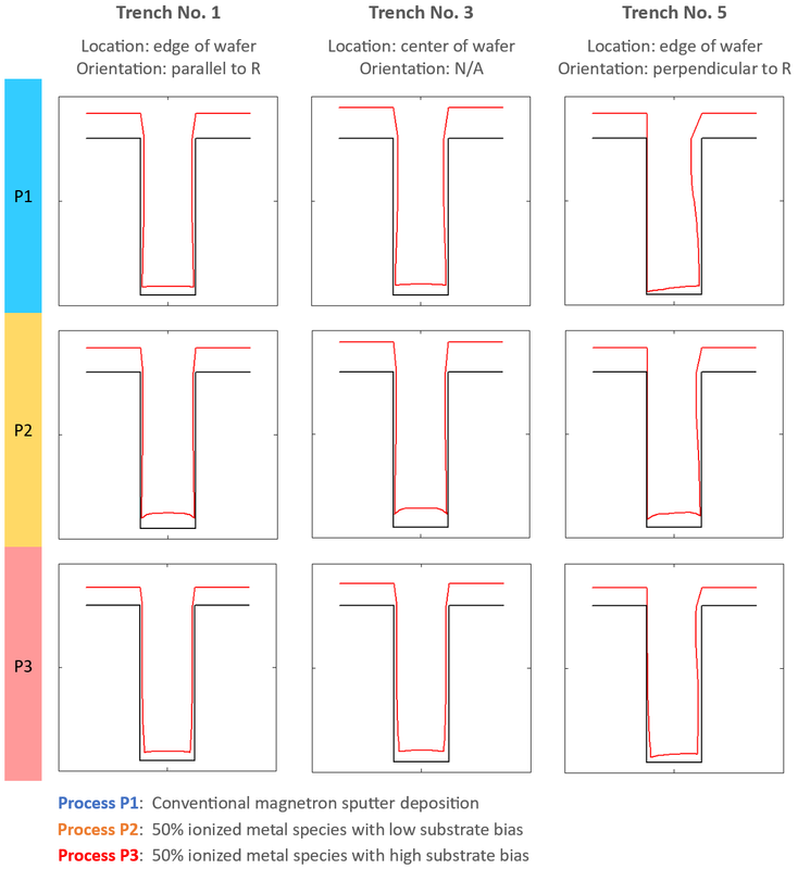
With a built model, we simulated coating profiles on the trench facets and their variation for different areas and trench orientations. The result (see diagrams for 3 trenches in 3 different processes) exhibits characteristics that are familiar to engineers and researchers:
1. Conventional sputtering builds thicker layers near the trench openings due to the shadowing of large-incident-angle vapor components.
2. Ionized and sheath-collimated metal species (via RF excitation) reduces the overhang and produces thicker layers on trench bottoms; they do not, however, enhance the coverage of trench walls.
3. Re-sputtering of metal from trench bottoms, through application of a high bias, can greatly enhance the coverage of trench walls.
4. Trenches that are near the wafer edge and are perpendicular to the radius have poorer coverage despite the use of a large-area target and energized ion species.
Armed with numerical models of this type, one can study and optimize a trench-lining process with considerable ease and shorten the time of development by reducing the need of hardware trials. For example, a simulation may point out an optimal ionization ratio for metal vapor in a specific geometry. The model may also lead to a more symmetric wall coverage for trenches that are located near the wafer edge and perpendicular to the radius.
We would like to hear your feedback on this subject. Please contact us at Tin Model LLC.
Copyright © 2025 Tin Model LLC. All rights reserved.