Tin Model special announcement, March 24, 2025
Breakthrough Trench-Lining Technology for Semiconductor Manufacturing
Tin Model LLC proudly announces its latest innovation: PVD trench-lining method for the semiconductor Damascene processes.
Tin Model's technology is an alternative to today's predominant method that employs specialty equipment and is expensive to operate. Tin Model's technology achieves the long-sought objectives in semiconductor manufacturing:
1. Reliable lining of high-aspect-ratio trenches and vias.
2. Uniform trench lining across large semiconductor wafers.
3. Symmetric coverage regardless of trench orientations (including peripheral areas).
4. Applicable to metals and non-metals.
5. Modular and compatible with cluster-tool configurations.
6. Scalable from current to next-generation nodes.
Tin Model's method can be used for deposition of diffusion barrier, adhesion layers and seed layers for copper interconnects. Tin Model’s method is low cost in both equipment and processing.
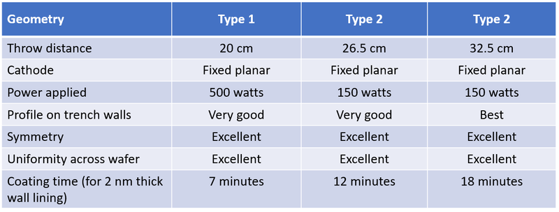
*Values in the table are for a 20-cm diameter wafer, as an example.
The aim of the innovation is to increase the yield and lower the cost of manufacturing where trench lining is crucial. Tin Model’s technology is patent pending and available for licensing. Please contact us for further information.
Copyright © 2025 Tin Model LLC. All rights reserved.